Learn about chip stacking, GPU memory bandwidth, and HBM4 specs.
DRAM vs. HBM: Breaking the AI Memory Bottleneck in 2026
The rapid evolution of Artificial Intelligence (AI) has brought the computing world to a critical crossroads. While processing power—measured by trillions of operations per second—has skyrocketed, a silent crisis has emerged: the "Memory Wall." In 2026, the primary constraint for Large Language Models (LLMs) and generative AI is no longer just how fast a chip can "think," but how quickly it can be fed data.
This technical deep dive explores the fierce competition between traditional DRAM and HBM (High Bandwidth Memory), detailing why standard memory architectures are hitting a physical ceiling and how next-generation HBM technology is dismantling these bottlenecks.
The Evolution of the Memory Crisis
For decades, the industry relied on standard Dynamic Random Access Memory (DRAM). Whether in the form of DDR5 for servers or LPDDR5X for edge devices, these technologies served us well. However, the rise of "Massive AI Workloads" has fundamentally changed the VRAM requirements for modern hardware.
Why Traditional DRAM is Failing AI
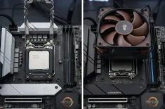
Traditional DRAM (like DDR5) communicates with the processor via long, narrow pathways on a PCB (Printed Circuit Board). This architecture faces three terminal issues:
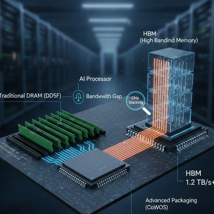
- The Bandwidth Gap: A standard DDR5 module might offer a memory bandwidth of around 50-60 GB/s. In contrast, an AI model like GPT-5 or its 2026 successors requires bandwidth in the terabytes per second (TB/s) to keep GPU memory from sitting idle.
- Physical Footprint: To get more capacity with traditional DRAM, you must add more DIMM slots, which take up massive amounts of "real estate" on a motherboard. In a data center, space is at a premium.
- Power Inefficiency: Moving data across a motherboard requires significant voltage to overcome electrical resistance. As AI workloads scale, the energy cost of simply moving data becomes higher than the cost of processing it.
Enter HBM: The Solution to the Bottleneck
HBM (High Bandwidth Memory) was designed specifically to bypass these limitations. Instead of placing memory chips side-by-side on a board, HBM utilizes chip stacking to build "skyscrapers" of memory directly next to the processor.
How HBM Solves the Bandwidth Limitation
The breakthrough of HBM lies in its verticality and proximity. By using Through-Silicon Vias (TSVs)—tiny vertical wires that poke through the silicon layers—HBM creates an incredibly wide interface.
- Ultra-Wide Interface: While a standard DRAM channel is 64 bits wide, an HBM3e or HBM4 stack uses a 1024-bit or 2048-bit interface. This allows for a massive "firehose" of data.
- Reduced Latency: Because the HBM stacks are co-packaged with the GPU on a single interposer, the physical distance data travels is measured in millimeters rather than centimeters.
- HBM4 and the 2026 Standard: As of early 2026, the transition to HBM4 has introduced "Logic Base Dies." For the first time, the bottom layer of the memory stack is built on a logic process (like 5nm), allowing the memory to perform basic data pre-processing before it even reaches the GPU.
Comparison: DRAM, LPDDR5X, and HBM
While HBM is the king of the data center, other technologies like LPDDR5X play a vital role in the "AI PC" and smartphone era of 2026.
| Feature | DDR5 (DRAM) | LPDDR5X | HBM3e / HBM4 |
|---|---|---|---|
| Primary Use | General Servers / PCs | Smartphones / AI Laptops | AI Accelerators |
| Max Bandwidth | ~60 GB/s (per DIMM) | ~100 GB/s | 1.2 TB/s - 2.0 TB/s |
| Form Factor | Large DIMM Slotted | Soldered on Board | Chip Stacking (Integrated) |
| Efficiency | Low | High (Low Power) | Extreme (Short Traces) |
The "Memory Wall" and Advanced Packaging
The true hero of 2026 AI hardware isn't just the memory itself, but the advanced packaging that enables it. Technologies like TSMC’s CoWoS (Chip-on-Wafer-on-Substrate) allow manufacturers to fuse the GPU and HBM stacks into a single, high-performance unit.
This integration is the only way to meet the soaring VRAM requirements of trillion-parameter models. Without HBM, the GPU memory would become a "traffic jam," where the processor's cores spend 90% of their time waiting for data to arrive from the DRAM.
Key Insight: In 2026, memory is no longer a "storage bin"—it is an active component of the compute engine. The shift from 2D (flat) to 3D (stacked) architectures has effectively saved Moore's Law from obsolescence.
Future Outlook: Beyond 2026
As we look toward the end of the decade, the industry is already moving toward HBM4E and even "Processing-in-Memory" (PIM), where AI calculations happen inside the memory layers themselves. This will further reduce the AI memory bottleneck, allowing for real-time, on-device intelligence that was previously impossible.
For enterprises and developers, understanding the distinction between HBM (High Bandwidth Memory) and traditional DRAM is essential. If your goal is to train or deploy cutting-edge AI, the quality and speed of your memory are now just as important as the number of teraflops in your processor.